S1E12 Chatshaala with electronics gadgets | PCB Layout using KiCAD

  • Links to recordings: here
  • Here is the room link to join: chaatshala
  • Timings: Mo-Fr 11:00AM to 12:30PM

Today we explored the followings:

KiCAD : The Open Source software for designing Schematic and PCB Layout.

Designed PCB Layout of simple power supply in PCB Layout Editor of KiCAD.

  • Open PCB Layout Editor
  • Update PCB from Schematic
  • Load Netlist
  • Placing Components on top layer
  • Routing bottom layer
  • Darwing Edge for dimension
  • Adding text to the PCB silkscreen
  • Viewing 3D model for the PCB

[center]

[/center]

You can also post your question and discuss in this thread.

Happy Exploring!

3 Likes

Some 3d models of components are not visible above. Probably some libraries not installed, or the foot prints used did not have a 3d model.

Here is my pcb 3d view. My connector does not have a 3d model, hence it is rendered only as a silk screen foot print.

3 Likes

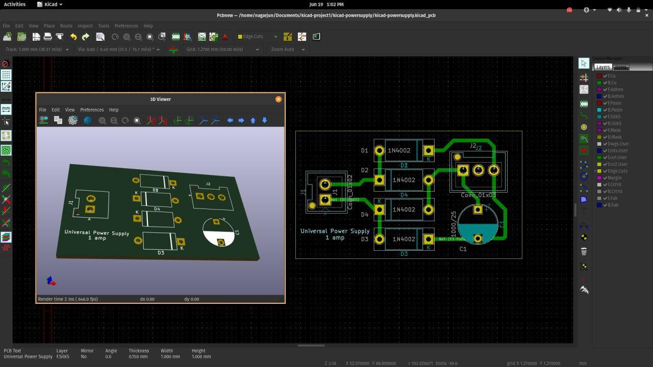
With Kicad one can view the 3d in realtime as one places components. This is very useful if one has a cad design for housing. We can add the housing as a custom part and place the PCB inside, then move components in realtime.

3 Likes

I could not log back in, once I logged out during the session. :frowning:

Nevertheless, watched the recording later on. :+1: 
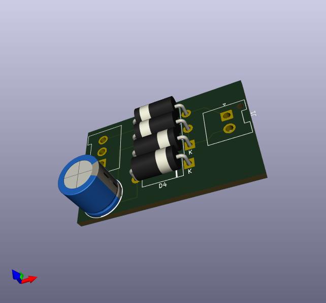
Ashish showed a ‘handmade’ PCB. Thanks Ashish! :slight_smile:

3 Likes

Saw that the traces have to be hand-routed in KiCAD, Does KiCAD provide autorouting, the way Eagle does?

3 Likes

Kicad does not have autorouter. But it has a push and shove router. IE it will move existing tracks, adhering to your set design rules, as you try to add a track. If it cannot move traces it will find a new shortest path. If it cannot do either it will lay a track upto the point it can and then stop.

2 Likes